INDUCTOR
The symbol for a Inductor is L .The name of a Inductor must start with L, and it takes the following general form
L(name)N+ N- LNAME LVALUE IC=Vo
N+ is the positive node and N- is the negative node. The voltage of node N+ is assumed positive with respect to node N-, and the current flows from node N+ through the Inductor to node N-. LNAME is the model name, and LVALUE is the nominal value of the Inductor, IC defines the initial (time zero) current of the Inductor, Io.
If LNAME is omitted, LVALUE is the Inductance in Henrys, and the LVALUE can be positive or negative but must not be zero.
MODEL PARAMETERS FOR INDUCTORS
Name Meaning Units Default
L Inductance multiplier 1
IL1 Linear Current Co efficient Amps -1 0
IL2 Quadratic Current Co efficient Amps -2 0
TC1 Linear Temperature Co efficient °C -1 0
TC2 Quadratic Temperature Co efficient °C -2 0
IND=LVALUE * L * (1+IL1*I+IL2*I2
* [1+TC1 * (T – To) + TC2 * (T – To) 2 ]
where T is the operating temperature in degrees Celsius ,and To is the room temperature in
degrees Celsius.
Note:- L is an inductance multiplier, rather than the value of the inductance .It scales the actual inductance value .LVALUE ,thus ,L=1.1 means that LVALUE is multiplied by 1.1,not that LVALUE is 1.1H
Some Inductor statements
L1 6 5 10MH
LLOAD 12 11 5UH IC=0.2MA
LLINE 15 14 ACAP 5MH
LCHOKE 20 19 ACAP 20NF IC=0.5MA
.MODEL LMOD IND (L=1 IL1=0.1 IL2=0.002 TC1=0.02 TC2=0.005)

Custom Search
Friday, July 18, 2008
CAPACITOR parameters - pspice
CAPACITOR
The symbol for a capacitor is C .The name of a capacitor must start with C, and it takes the following general form
C(name)N+ N- CNAME CVALUE IC=Vo
N+ is the positive node and N- is the negative node. The voltage of node N+ is assumed positive with respect to node N-, and the current flows from node N+ through the capacitor to node N-. CNAME is the model name, and CVALUE is the nominal value of the capacitor, IC defines the initial (time zero) voltage of the capacitor, Vo.
If CNAME is omitted ,CVALUE is the capacitance in farads ,and the CVALUE can be positive or negative but must not be zero .
MODEL PARAMETERS FOR CAPACITORS
Name Meaning Units Default
C Capacitance multiplier 1
VC1 Linear Voltage Co efficient Volt -1 0
VC2 Quadratic Voltage Co efficient Volt -2 0
TC1 Linear Temperature Co efficient °C -1 0
TC2 Quadratic Temperature Co efficient °C -2 0
C is a capacitance multiplier, rather than the value of the capacitance .It scales the actual capacitance value .CVALUE ,thus ,C=1.1 means that CVALUE is multiplied by 1.1,not that CVALUE is 1.1F
Some Capacitance statements
C1 6 5 10UF
CLOAD 12 11 5PF IC=2.5V
CINPUT 15 14 ACAP 10PF
C2 20 19 ACAP 20NF IC=1.5V
.MODEL ACAP CAP (C=1 VC1=0.01 VC2=0.002 TC1=0.02 TC2=0.005)
variables and their meanings in PSPICE
Voltage Output
For DC Sweep and Transient Analysis, the output voltages can be obtained by the following statements:
VARIABLES MEANING
V(5) Voltage at Node 5 with respect to Ground
V(4,2) Voltage of Node 4 with respect to Node2
V(R1) Voltage of Resistor R1,where the first Node(as defined in the circuit file) is positive with respect to the second Node.
V(L1) Voltage of Inductor L1,where the first Node(as defined in the circuit file) is positive with respect to the second Node.
V(C1) Voltage of Capacitor C1,where the first Node(as defined in the circuit file) is positive with respect to the second Node.
V(D1) Voltage across Diode D1,where the first Node is positive with respect to the cathode.
Current Output
For DC Sweep and Transient Analysis, the output currents can be obtained by the following statements:
VARIABLES MEANING
I(VS) Current Flowing into DC Source Vs.
I(R5) Current Flowing into Resistor R5,where the Current is assumed to flow from the first Node(as defined in the Circuit file )through R5 to the second Node.
I(D1) Current into diode D1.
IA(T1) Current at Port A of Flowing in to DC Source Vs.
symbols for two terminal elements - pspice
SYMBOLS FOR TWO TERMINAL ELEMENTS
C Capacitor
D Diode
E Voltage Controlled Voltage Source
F Current Controlled Current Source
G Voltage Controlled Current Source
H Current Controlled Voltage Source
I Independent Current Source
L Inductor
R Resistor
V Independent Voltage Source
C Capacitor
D Diode
E Voltage Controlled Voltage Source
F Current Controlled Current Source
G Voltage Controlled Current Source
H Current Controlled Voltage Source
I Independent Current Source
L Inductor
R Resistor
V Independent Voltage Source
Thursday, July 17, 2008
Operating Temperature - PSPICE
OPERATING TEMPERATURE
(Command: .TEMP) in degrees Celsius °C.
The operating temperature of an analysis can be set to any desired value by the .TEMP command .The general form is,
.TEMP { (one or more temperature) values } [default 27 °C]
Some temperature statements
.TEMP 50
.TEMP 25 50
.TEMP 0 25 50 100
(Command: .TEMP) in degrees Celsius °C.
The operating temperature of an analysis can be set to any desired value by the .TEMP command .The general form is,
.TEMP { (one or more temperature) values } [default 27 °C]
Some temperature statements
.TEMP 50
.TEMP 25 50
.TEMP 0 25 50 100
Wednesday, July 16, 2008
Program for analysis of three phase circuit representing generator transmission line and load - PSPICE
The aim of the program is to analyze the three phase circuit representing generator transmission line and load and to plot 3 phase current and neutral current.
Problem:
220v, 50hz supply is applied to
a) balanced 3-phase star connected load contains 25 ohms of resistance and 6mH of inductance in each phase
b)
Un-balanced 3-phase star connected load of 10 ohms, 3mH inductance, 20ohms, 4mh & 30 ohms , 5mh inductance for 3-phase respectively. Plot 3 phase currents and neutral laod. If source L is 6mH and value of neutral inductance is 7mH
PROGRAM CODE ( for balanced 3-phase analysis )
*balanced 3-phase analysis
*source description
VS1 1 2 SIN(0 220 50HZ 0 0 0DEG)
VS2 1 4 SIN(0 220 50HZ 0 0 120DEG)
VS3 1 6 SIN(0 220 50HZ 0 0 240DEG)
VS4 10 9 DC 0V
VS5 10 11 DC 0V
VS6 10 13 DC 0V
VS7 0 10 DC 0V
*COMPONENT DESCRIPTION
L1 2 3 6M
L2 4 5 6M
L3 6 7 6M
L4 1 0 6M
L5 8 3 6M
L6 14 5 6M
L7 12 7 6M
R1 8 9 25
R2 12 11 25
R3 14 13 25
* ANALYSIS DESCRIPTION
.TRAN 20ms 160ms
*OUTPUT DESCRIPTION
.PROBE
.END
OUTPUT

PROGRAM CODE ( for Un-balanced 3-phase analysis )
*unbalanced 3-phase analysis
*source description
VS1 1 2 SIN(0 220 50HZ 0 0 0DEG)
VS2 1 4 SIN(0 220 50HZ 0 0 120DEG)
VS3 1 6 SIN(0 220 50HZ 0 0 240DEG)
VS4 10 9 DC 0V
VS5 10 11 DC 0V
VS6 10 13 DC 0V
VS7 0 10 DC 0V
*COMPONENT DESCRIPTION
L1 2 3 6M
L2 4 5 6M
L3 6 7 6M
L4 1 0 6M
L5 8 3 3M
L6 14 5 4M
L7 12 7 5M
R1 8 9 10
R2 12 11 30
R3 14 13 20
* ANALYSIS DESCRIPTION
.TRAN 20ms 160ms
*OUTPUT DESCRIPTION
.PROBE
.END
OUTPUT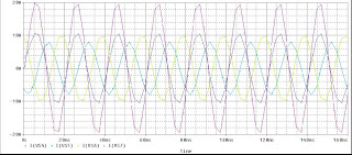

The format for a circuit file in PSPICE
The Format for a Circuit File is as follows:
Title
Circuit description
Analysis description
Output description
.End
Note:
1. First line is the title line, always in the first line only& it may be contain any type of text
2. Last line must be the .End command and it always in the last line only.
3. The order of remaining three lines is not important in sequence &does not affect the O/P results of Simulation.
4. In a statement if more than one line, the statement can be continue on the next line,
a continuation line is identified by a(+)sign in the first column of the next line.
The continuation line must follow one another in the proper order.
5. P Spice comments or statements can be in either upper case or lower case.
6. In P Spice the symbols are represented with out subscripts Ex:-Vs =VS , Is =IS , R1 =R1 ,
Subscribe to:
Posts (Atom)
